English 


Views: 0 Author: Site Editor Publish Time: 2021-04-23 Origin: Site

Nowadays, LEDs are getting brighter and brighter. In order to meet the needs of the general lighting market, LEDs must match the lumen output of traditional incandescent lamps and halogen bulbs (usually within the same size range), and this task is also a thermal challenge.
Common high-brightness (HB) LEDs can only convert about 45% of the energy into light, and the rest appears as heat. This heat needs to be removed from the LED as quickly as possible to prevent the LED from overheating and potentially catastrophic failure. The increased power input of this HB LED accelerates more power into the LED, which in turn generates more heat.
This situation is a challenge facing LED manufacturers, and there are many different ways to overcome it on the market. Everything starts with the LED package, because the package provides many functions: it not only provides physical protection for the LED chip, and fixes the LED on the lamp, but it also means that the LED chip is in a sealed package environment, which greatly The heat dissipation caused by convection and radiation is prevented, and the LED can only be dissipated by heat conduction from the back of the package.
In this case, the use of a thermally conductive substrate can help narrow the heat transfer path between the LED and the heat sink. But it may be easier to use copper sheet materials, because copper has very good thermal conductivity. The thermally conductive substrate needs to be electrically insulated, because it also needs to carry copper rails that deliver power to the LED. If the medium is not insulated, the LED will be short-circuited. Therefore, materials that can conduct heat and insulate are needed.
LED manufacturers continue to research solutions to reduce costs, either by eliminating processes or using more cost-effective materials. The ultimate goal is to reduce the overall cost of LED bulbs to a level that consumers can buy at a low price.
Package selection
There are generally two methods for HB LED packaging.
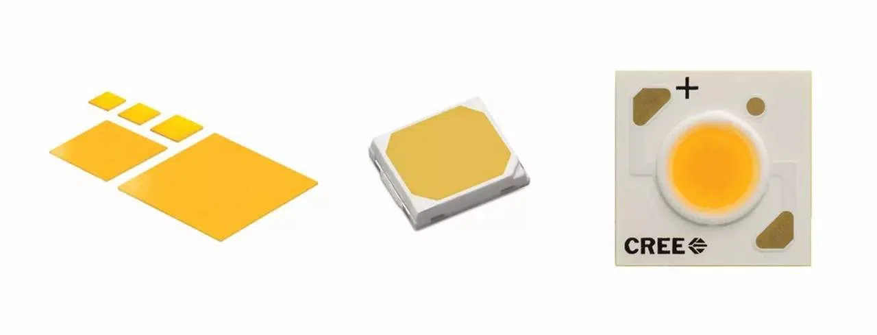
Manufacturers can integrate a single large LED chip or chip set (for example, one red, one green and one blue) using surface mount technology (SMT), or the manufacturer can package some chips directly onto the PCB-COB. Figure 1 includes samples of different package types from manufacturers Cree, Lumileds and Samsung.
Figure 1 Samsung chip scale package (CSP) device (left);
Lumileds' mid-power LED (middle); Cree's COBLED (right)
On the surface, COB LED is very simple. By packaging the bare LED chips directly onto the PCB, this clearly makes COB equipment a more cost-effective choice.

The disadvantage of COB LEDs is that they tend to have a wide angle. These can be used in lighting fixtures such as street lights and high bay lights. But for directional beams, such as in car headlights or ceiling downlights, SMD directional high-power LED products are required.
Benefits of HB LED and ceramics
The key requirement for directional HB LED packaging is that both sides of the package substrate need to be "circuited", and copper rails pass through the substrate to connect two sets of circuits. This is critical because the package substrate needs to be mounted on the module or lamp circuit. Vias filled with conductive copper are required, but these vias need to be isolated from the rest of the circuit. This underestimates materials such as metal core PCB (MCPCB).
So far, the only market material that can meet this requirement is electronic ceramics. Ceramics are ideal because it is a natural dielectric, and certain types of ceramics are excellent thermal conductors. The through holes drilled into the substrate will be electrically isolated from the rest of the material.
Ceramics are a good choice, and another reason is that they can pass through the very high resolution Direct Copper Plating (DPC) process. DPC is an additive process in which copper traces are sputtered onto the ceramic to build a circuit instead of using a reduction process. This process adds copper very accurately, measuring with micron accuracy.
This is where the low-cost MCPCB fails again. In order to make a dielectric layer for MCPCB, epoxy resin needs to be added and the copper circuit is glued to the surface of the metal core. It is this epoxy resin layer that acts as a dielectric, which is usually mixed with ceramic particles to improve thermal performance. This can only be done through a reduction process, so once again, ceramics become the only choice.
